Research and facilities
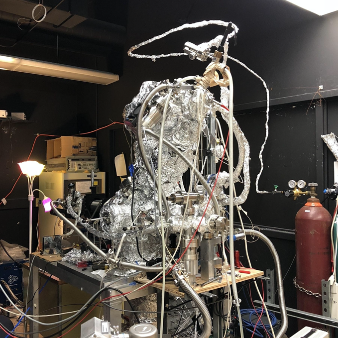
We have many facilities, like Scanning Tunnel Microscopy / Spectroscopy, Molecular Beam Expitaxial, Laser Spectroscopy and time-resolved ARPES. Most our research topics are based on these equipments.
Research Topics
Intrinsic magnetic topological insulator
In intrinsic magnetic topological insulators, Dirac surface-state gaps are prerequisites for quantum anomalous Hall and axion insulating states. Unambiguous experimental identification of these gaps has proved to be a challenge. Here in our group, Hyunsue Kim has successfully grown the expitaxial MnBi2Te4 (MBT) on graphene and graphite substrates using MBE. By conducting layer dependent study of MBT using STM, the interplay between the dirac mass gap and its intrinci magnetism has been unambiguously investigated by Mengke Liu.
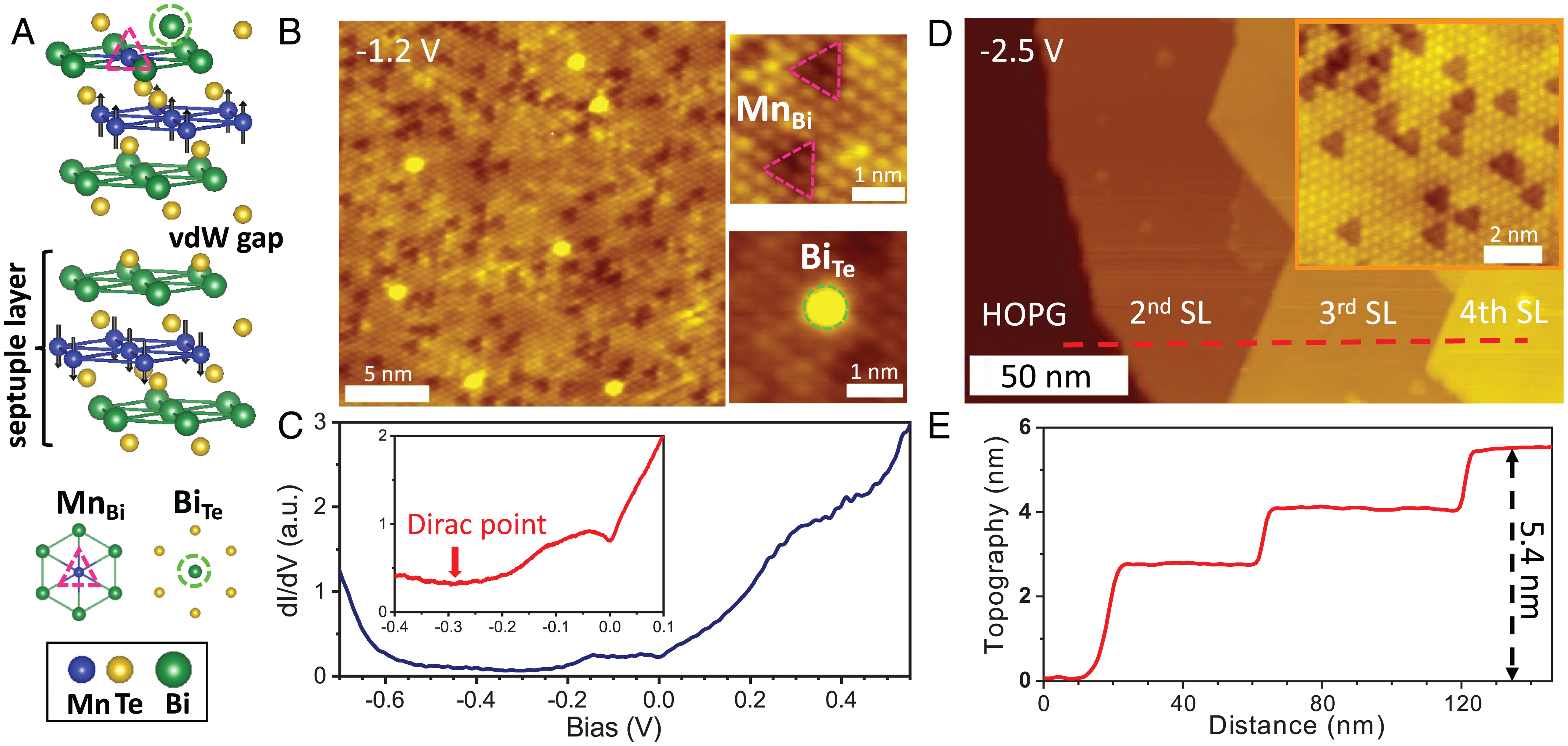
MBT bulk v.s. MBE thin films (M. Liu et al. PNAS (2022))
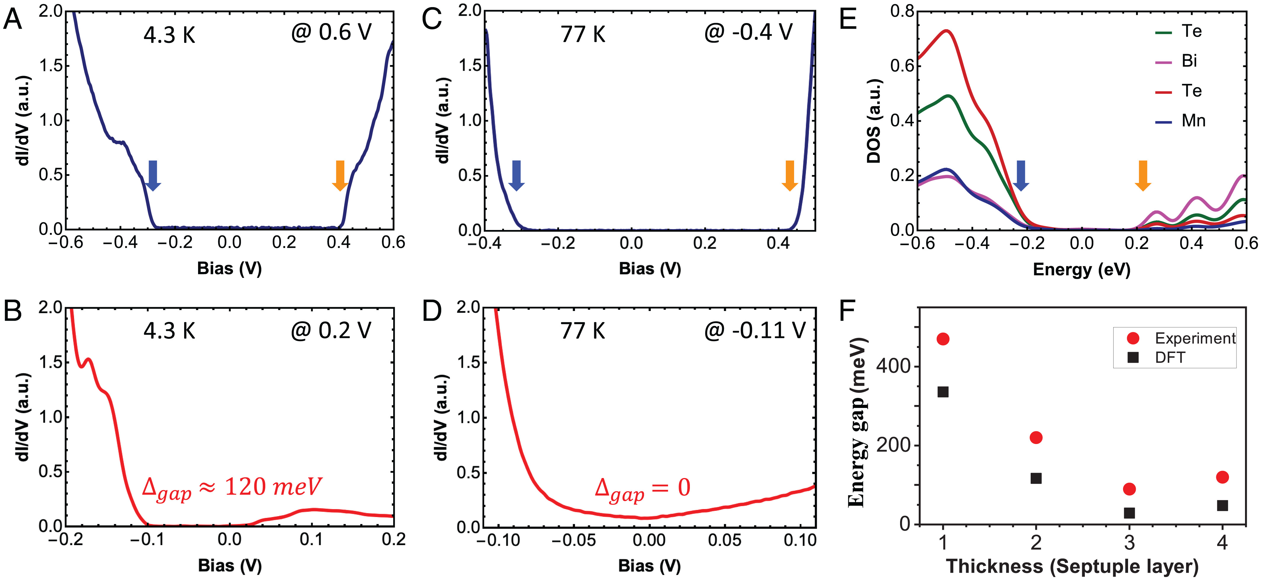
Direct observation of Dirac mass gap (M. Liu et al. PNAS (2022))
Twisted 2D materials: Moire quasicrystals and commensurate moire crystals at large twist angles
Using valley-resolved scanning tunneling spectroscopy, the mutual Umklapp scatterings and coherent valley couplings are studied in the twisted WSe2 moire quasicrystal (at 30-degree) and commensurate moire crystal (at 21.8-degree). In particular, the K-valley shows rich electronic structures exemplified by the formation of mini-gaps near the valence band maximum. These discoveries demonstrate that bilayers with large twist angles offer a design platform to explore moiré physics beyond those formed with small twist angles.
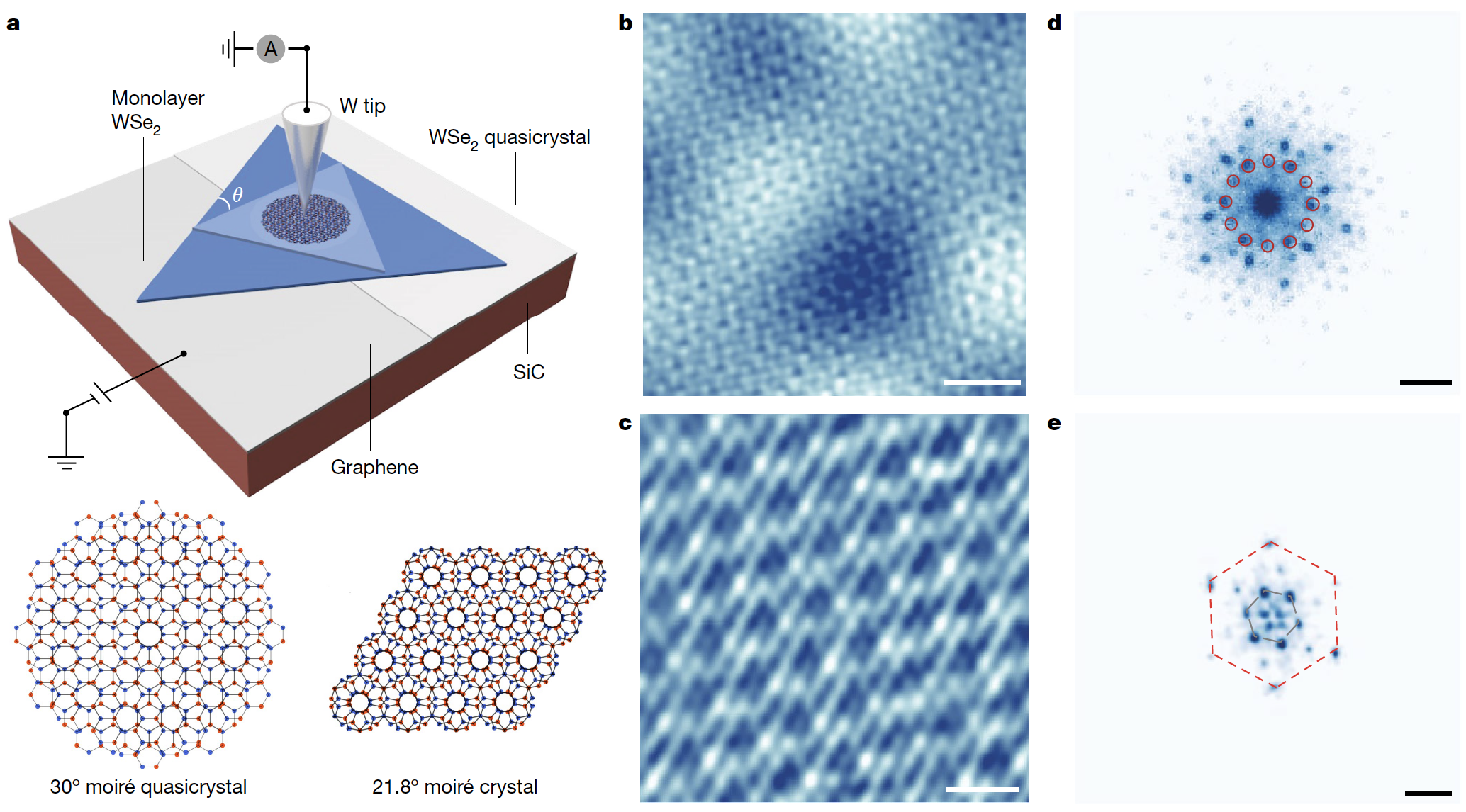
Moire crystal and moire quasicrystal (Li, Y., et al. Nature (2023))
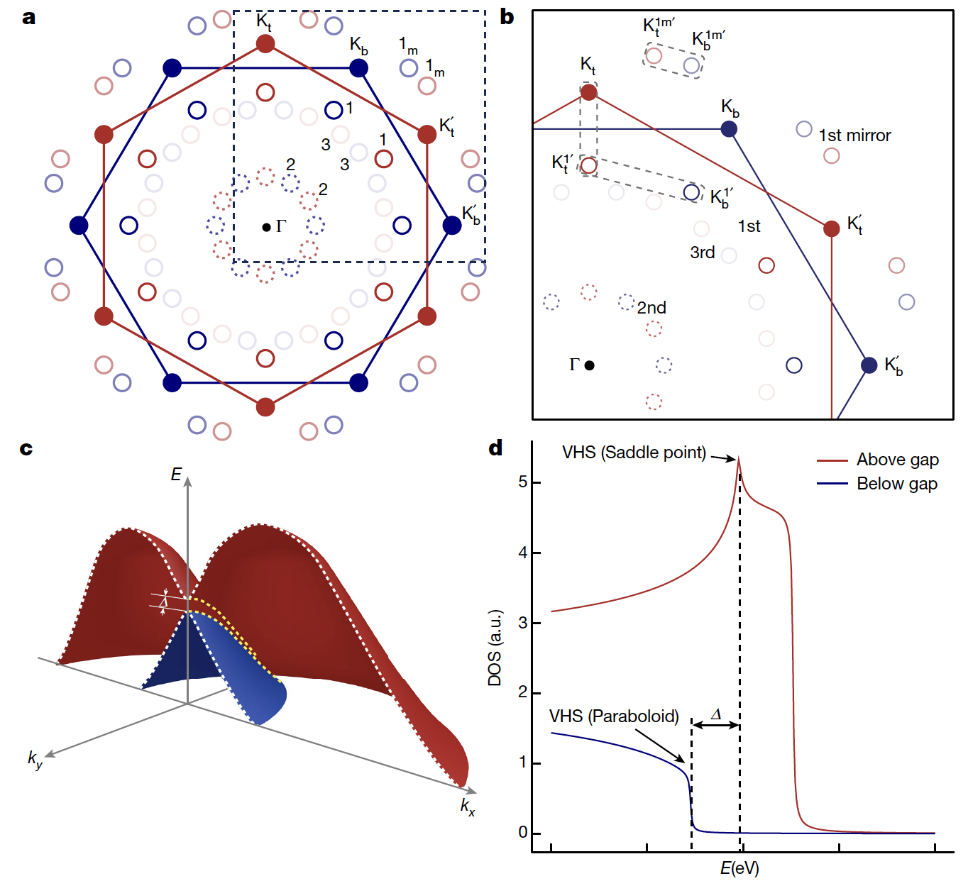
Umklapp scatterings in moire quasicrystal (Li, Y., et al. Nature (2023))
Time-solved ARPES study of 2D Ag as a large indirect gap semiconductor
2D materials have intriguing quantum phenomena that are distinctively different from their bulk counterparts. Recently, epitaxially synthesized wafer-scale 2D metals, composed of elemental atoms, are attracting attention not only for their potential applications but also for exotic quantum effects such as superconductivity. By mapping momentum-resolved electronic states using time-resolved and angle-resolved photoemission spectroscopy (ARPES), we reveal that monolayer Ag confined between bilayer graphene and SiC is a large gap (>1 eV) 2D semiconductor.
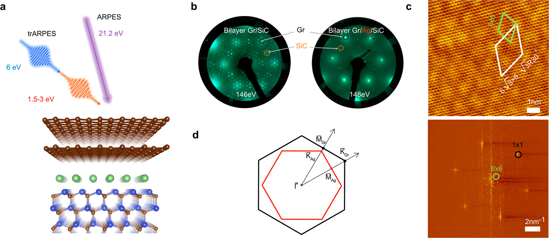
Monolayer Ag atomic structure and surface characterization.(W. Lee et al. Nano Letters(2022))
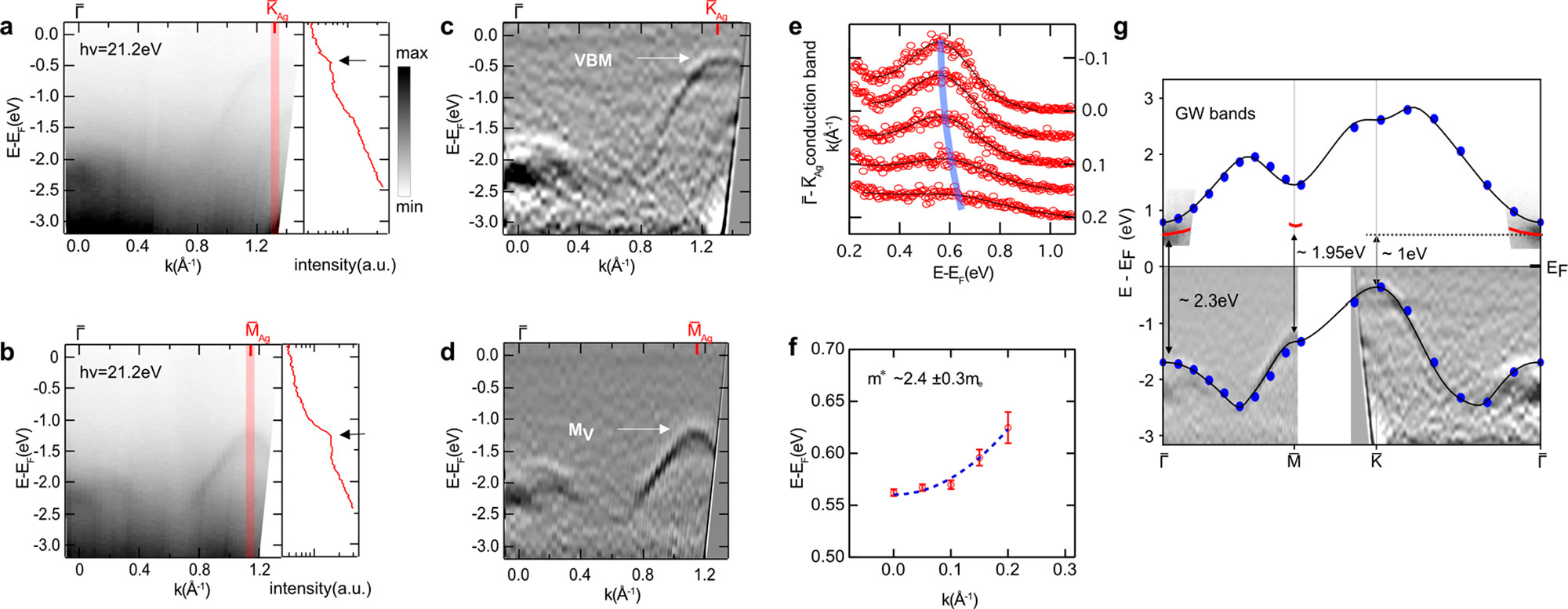
Occupied and unoccupied electronic structures of monolayer Ag.(W. Lee et al. Nano Letters(2022))
Facilities
ARPES
Our ARPES system consists of SCIENTA R3000 analyzer, home-built sample manipulator, UHV Prep chamber and pumps for UHV. Home-built sample manipulator has 6 axes degree of freedom and a cooling ability upto near liquid nitrogen temperature. Prep chamber is made up of a heater, thermocouple and ion gauge so that it is possible to treat samples before measurement. Furthermore, we are using a helium discharge lamp as a beam source.
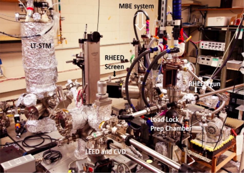
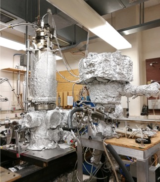
Low temperature STM, LEED, CVD, and MBE cluster
This cluster of instruments enables growth and in-situ measurement capabilities. The MBE chamber is used for growth of atomically flat, epitaxial Ag(111), as well as Al capping layers. The MBE also equipped with a RHEED for in-situ characterization. There is a UHV prep chamber for transferring samples from atmosphere. The LEED chamber is also includes a sputter gun, an e-beaming stage, and growth capabilities of PVD of hBN and MBE of BeO. Finally, a low temperature STM is used for in-situ characterize the samples. This entire cluster was home-built, and the system is used for a variety of studies characterizing the structure and electronic properties of 2D materials.
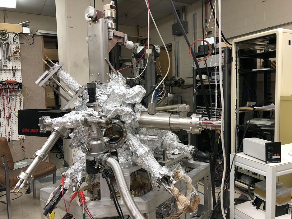
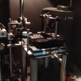
Home-built low temperature STM & MBE growth chamber
MBE chamber can be easily connected to STM chamber, which makes in-situ measurement quick and simple. Project on this system mainly focus on 2D metallic thin film and superconductivity. Please see our RSI paper for more information:
Kim, J., et al. (2015). "Compact low temperature scanning tunneling microscope with in-situ sample preparation capability." Review of Scientific Instruments 86(9).
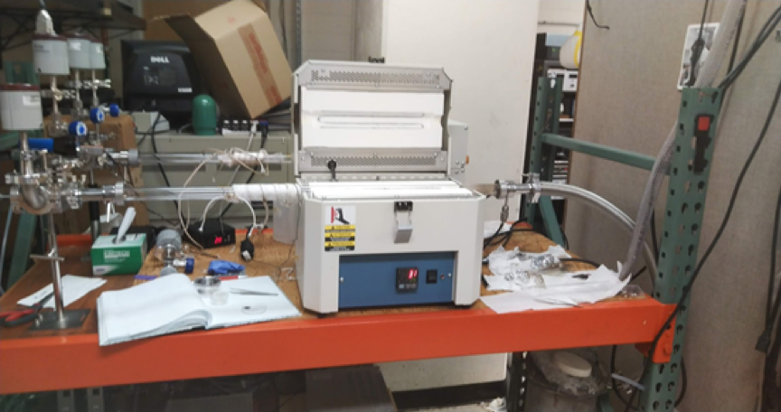
Molecular Beam Expitaxial
This home-built MBE system has a capability to grow different TMDs, topological insulators and metal thin films. The system equipped with a RHEED for monitoring growth status and different pumps for UHV.
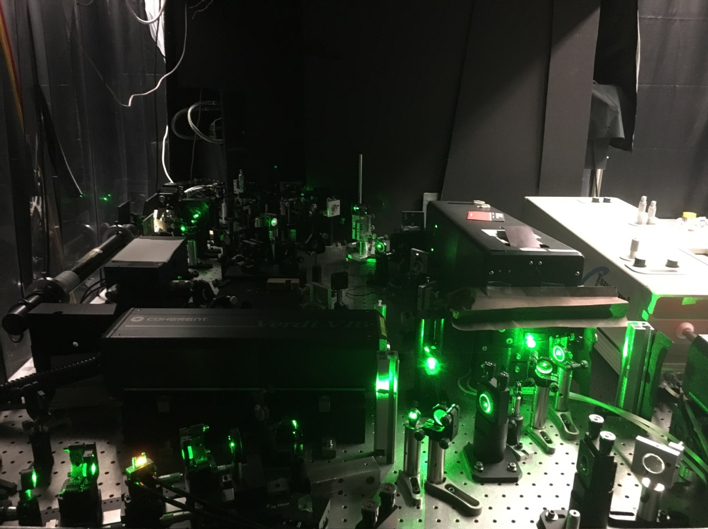
Ultrafast mode-locked Ti:Sapphire laser systems
Ultrafast lasers provide short laser pulses of 20-160 fs with tunable wavelength from 700 nm to 950 nm. These lasers are excitation sources for time-resolved measurements and nonlinear optics such as time-resolved PL, transient reflection and SHG spectroscopies.

Room-temperature back-scattering optical microscope
It is capable of PL, Raman, DR and SHG measurements at room temperature.
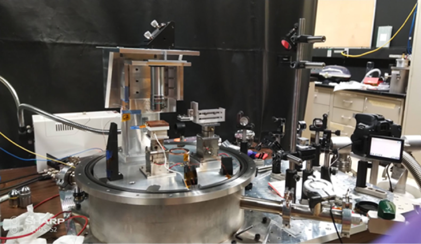
Vacuum transfer system
It is a homebuilt facility. We use this system to prepare vertical van der Waals heterostructures in vacuum for avoiding the air bubble.
Low temperature microscope spectroscopy with closed-cycle cryostat
We can measure photoluminescence, Raman, nonlinear optics spectroscopy and et. al. at 4K environment.
Chemical vapor deposition
We use this facility to grow transition metal dichalcogenide monolayers (such as WS2, MoS2, Wse2 and MoSe2) or heterostructure.